2.2 Components of a Flame Atomic Absorption/Emission Spectrometer System
2.2.9 Detectors
AAS and AES measurements require that the energy contained in a photon to be converted into a measurable electrical signal. Early detectors relied on a more solid-state version of the photoelectric effect that is best illustrated by a phototube, one of the first detectors to convert radiant energy to electrical energy.
Phototubes: Figure 2-6 shows a diagram of a basic phototube (PT). A PT consists of an evacuated glass or quartz chamber containing an anode and a cathode. Cathode surfaces are composed of materials that readily give up electrons; Group I metals such as Cs work well of this purpose. A relatively large potential is placed across the anode and cathode, usually 90V, and the gap is referred to as a dynode. Electrons contained in the cathode are released as photons with a sufficient energy strike the surface. This causes electrons to move through the low-pressure gap to the anode, which produces a current. For a PT, a single photon causes only a single electron to be measured. For emission spectroscopy, the magnitude of current produced by the cascade of electrons in the detector is directly proportional to the concentration of analyte in the sample.
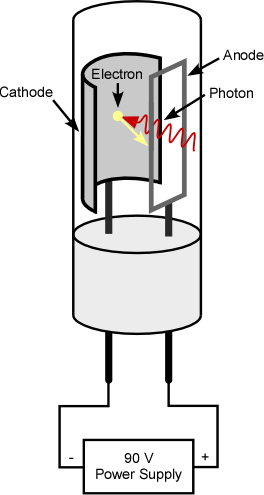
Figure 2-6 Diagram of a Phototube.
Photomultiplier Tubes: Photomultiplier tubes (PMT) are an extension of the phototube where numerous dynodes are aligned in a circular or in a linear manner. Here most of the electrodes act as both an anode and a cathode with each dynode (electrode pair) having a potential difference of +90 V; thus, the potential increases by 90 V as an electron goes from one electrode to the next (refer to Animation 2.4 below). When nine dynodes are used, a common feature in PMTs, the net result is a yield of 106 to 107 electrons from a single emitted photon. This causes considerable amplification of a weak signal compared to a photon tube that does not amplify the signal. PMTs were excellent detectors for FAAS and FAES measurements due to the low intensity of radiation in these systems and have dominated these instruments for decades.
In Animation 2.3 below, only discrete packets photons are shown entering the detector from a chopped signal; this is only for illustration purposes since the stream of photons and the generated electrons are continuous producing an analog signal. Photons enter through a slit, strike the first cathode that is positively charged and a small number of electrons are produced. These electrons jump the gap to the next electrode where each arriving electron produces even more electrons due to the increased potential placed on the surface. This process is repeated over and over until a current is read at the anode (the final electrode). Play Animation 2.3 at this time.
Animation 2.3 Illustration of a Discrete Electron Multiplier.
Charge Coupled Devices: In the mid-1990s, a new style of photon detector (and collector) was developed and implemented into instruments because of advancements in computer chip technology that decreased cost of producing these chips. Before charge coupled devices (CCDs) can be understood and appreciated, the historical development of photosensitive computer chips must be presented.
The development of advanced detectors starts with a silicon diode device. A diode is an electronic device composed of two electrodes that can either act as a resistor or a conductor depending on the potential placed on the device. Such a device is shown in Figure 2.7a.
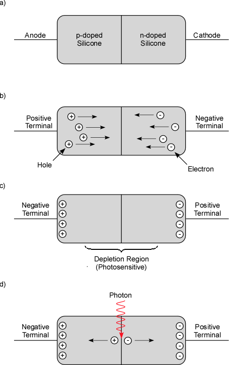
Figure 2.7 A Basic Silicon Diode. (a) with no applied voltage. (b) with a forward (positive) bias placed on the electrodes. (c) with a reverse (negative) bias placed on the electrodes. (d) the current generation resulting after a photon strikes the depletion region.
A silicon diode consists of two pieces of silicon, one positively doped (p-doped) and one negatively doped (n-doped), with the functional area (the depletion region) being at the interface between the two media. The positively doped end was created by doping (replacing) an occasional Si atom with a Group III element, such as aluminum. The net result is referred to as a positive charged carrier that can move through the chip, or an electron hole since one bond is missing between Al and Si. In contrast, the negatively doped end of a diode is a similar piece of silicon where occasional Si atoms have been replaced with a Group V element, such as phosphorus. The net result is the creation of a negatively charged carrier since this material contains extra electrons.
Combining the p-doped and n-doped silica into one device (called a pn junction) creates a diode that can be operated in two modes, forward and reverse bias. In the forward bias mode, a positive potential is placed on the p-doped semiconductor and a negative potential is placed on the n-doped semiconductor (refer to Figure 2.7b). This results in the holes and electrons moving toward the center of the device where they can combine and reduce the resistance in the diode; here the device acts as a conductor. The forward bias mode is of no interest in detectors utilized for spectrometry.
Figure 2.7c shows the silicon diode when a reverse bias is placed on the device. Here, the charges on the electrodes are reversed and the holes in the p-doped semiconductor are drawn toward the negative terminal while the electrons in the n-doped side are drawn toward the positive terminal. This results in the creation of a depletion area at the interface of the two semiconductors, where there are few holes or electrons in the matrix. As a result of the voltage barrier, high resistance is created which allows minimal electric current to cross the p-n junction; in this mode the device acts as a resistor. In this mode of operation, when a photon of sufficient energy (in the UV, visible, and near IR regions; photons with wavelengths from 190 nm to 1100 nm) strikes the depletion region, holes and electrons are created that then migrate to their respective terminals generating a current (Figure 2.7d). The amount of current generated is directly proportional to the number of reactive photons striking the depletion region. Thus, these devices can be used in the detection and quantification of radiant intensity. Silicon diodes are more sensitive than the older vacuum-style phototubes but their performance is still poor when compared to PMTs described earlier (due to the lack of amplification). The advantage of a silicon diode is the large numbers that can be placed in a linear arrangement referred to as a linear diode array (LDA).
Linear Diode Arrays: A linear diode array allows the simultaneous detection of a wide number of wavelengths. When a linear diode array is utilized, UV or visible light is first separated by a monochromator and the separated wavelengths are aligned onto the surface of a linear diode array with a collimating mirror or lens. Figure 2-8 illustrates a section of a linear arrangement of up to 400 individual diodes. Each wavelength of interest is positioned on one of these many p-n junctions allowing the intensity of each wavelength to be measured simultaneously. The entire UV and visible spectrum can be measured with considerable wavelength resolution with one LDA.
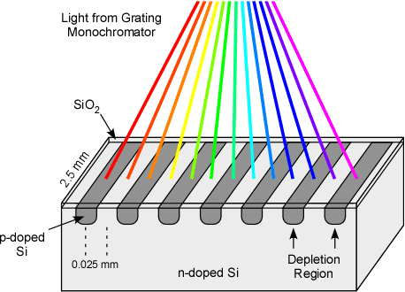
Figure 2-8 A Linear Diode Array. Each p-n junction, the interface between shaded regions, is a diode.
LDAs offer the advantage of measuring all wavelengths in a sample at the same time, which is especially important in emission spectrometry. This type of detector is commonly used today in instruments where detection limits are not a problem since LDAs do not amplify the original signal. Common uses include UV-visible detectors in inexpensive spectrometers and in many high performance liquid chromatography (HPLC) systems. The cost of production has greatly decreased in recent years and the cost of an LDA is now cheaper than a PMT, however PMTs have higher sensitivity, a larger dynamic range, and lower signal to noise ratios. In selecting between a LDA and a PMT detector one must weigh the benefit of simultaneous wavelength detection versus detection limit. LDA are most commonly used in absorption spectroscopy, but are not currently offered in common, more inexpensive FAAS or FAES systems. Diodes and linear diode arrays are mentioned here to aid in the understanding of charge–transfer devices, which are commonly used in AAS and AES today.
Charge-Transfer Devices: There are presently two types of charge transfer devices (CTDs), charge injection devices (CIDs) and charge coupled devices (CCDs). Both of these overcome the disadvantages of LDAs (low dynamic range, poor sensitivity, and low signal to noise ratios) by amplification (through timed storage or accumulation) of the original signal. As a result they can match the performance of PMTs and actually exceed them by simultaneous detecting multiple wavelength including separating different orders of diffraction. As a result of these advantages and due to the recent reductions in production costs and spatial constraints, CTDs are rapidly replacing PMTs.
CTDs are one- or two-dimensional arrays of detectors that can offer thousands of individual detector pixels. Both p-doped and n-doped semiconductors are used and individual pixels for each are shown in Figure 2-9.
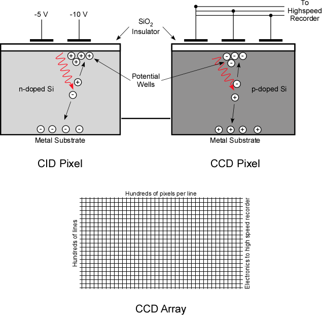
Figure 2-9 p-doped and n-doped pixel Charge Transfer Devices. (a) a Pixel for a Charge Injection Device (CID). (b) a pixel for a Charge Coupled Device (CCD). (c) an Array of CCDs (each pixel is a detector).
Charge injection devices (CIDs) use n-doped silicon (refer to Figure 2-9a). When a photon of sufficient energy strikes a bond in the silicon, a hole and an electron are created. The electron migrates to the positively charged substrate and is removed from the system. The hole migrates to a “potential well” that is created under the most negatively charged electrode. The system, as shown in Figure 2-9a acts as a capacitor because of the -5V and -10V applied potential. It is important to note that each “well” can accumulate between 105 to 106 charges per electron; this closely matches the performance (amplification) of PMTs discussed earlier. Note that the silicon and electrode are separated by a non-conductive silicon dioxide layer. After a sufficient amount of time (when a large number of holes have been created and collected) the applied electrical potential on the -5V electrode is removed and a voltmeter (potentiometer) is used to measure the capacitor potential under the -10V electrode. The capacitor potential is directly related to the number of holes collected. If sufficient counts are measured the holes are cleared from the CID and a new measurement is started. The advantage of CIDs is that counting can be continued by reestablishing the -5V connection. Thus, amplification of the signal, or more specifically accumulation of holes, can be completed in two ways, (1) by initially measuring a significant amount of time and (2) by measuring and deciding to continue the collection process. This process is non-destructive, thus, the accumulated signal can be read repeatedly until a desired magnitude is obtained. When placed in a 2-dimensional array, they can contain tens of thousands of pixels and each pixel can be positioned to collect data for a specific wavelength from the monochromator. Due to high thermal noise CIDs are usually cooled to liquid nitrogen temperatures.
Charge coupled devices (CCDs), invented in 1969 at Bell labs, are designed in an opposite manner as compared to CIDs. In CCDs, p-doped silicon is used and the electrodes atop the semi-conductive material are positively charged. An individual pixel for a CCD is shown in Figure 2-9b. Here, photons strike the doped silicon, holes are neutralized and removed by the metal substrate below the pixel and electrons migrate to the potential well where they are stored. Arrays are read from left to right by shifting the potential on the electrons and measuring the potential charges transferred between the electrodes. Again the system (each pixel) acts as a capacitor where its potential can be measured by removing the applied potential and measuring the capacitor potential with a voltmeter. An individual pixel consists of three electrodes (a three-phase clock circuit) that are used to sweep the charges to the right where they are moved to the next pixel and on to a high-speed shift register and then on to a preamplifier and readout. This allows for a pixel-by-pixel and row-by-row two-dimensional detector surface to be created. However, the measurement is destructive, unlike in CID detectors, so only one measurement is possible. This is not a disadvantage in FAAS or FAES measurements since a manual measurement only takes seconds to obtain, and doubling or tripling the reading time is relatively insignificant. For automated sample introduction, the increased data collection time is trivial. For most purposes, typical accumulations of the signal by CCDs match the amplification performance of PMTs.
For purposes of reference in spectrometry instruments, a CCD array (illustrated in Figure 2-9c) is about 1 cm by 1 cm in size and can contain up to approximately 20 000 pixels. Contrast this to the surface area needed to obtain the same resolution; one would have to position 20 000 PMTs at the proper angle with respect to the monochromator with each PMT being about 1.5 cm in diameter and 8 cm in height. The small size of the CCD array allows it to be placed inside the monochromator after a collimating mirror or lens and an exit slit is not required. Instruments with CCDs are significantly smaller in size, thus, less bench space is needed in the laboratory.
The two-dimensional nature of CCDs will be of more importance in the next chapter where inductively coupled plasma—atomic emission spectrometry (ICP-AES) is discussed. In ICP-AES, two dimensional reading devices are necessary to reduce interferences by allowing second and third diffraction orders that overlap in one dimension to be separated vertically onto the two dimensional array of a CCD.
As an interesting side note, CCDs are the imaging detector in older digital cameras, fax machines, advanced telescopes and many other imaging instruments. Here, like in spectrometry, an analog (continuous) signal is segmented into a digital or pixilated image. Arrays used in high-end (expensive) cameras can offer the same resolution as extremely low ASA rated emulsion camera films. The array can contain millions of pixels and a color grid on the array allows for color photography. As soon as an analytical instrument is placed into production, development of the next model is underway. For example, CCDs, a remarkable detector in advanced FAES instruments will soon be replaced by complementary metal oxide semiconductors (CMOS) detectors. The limitations of CCDs are the time requirements for amplification and the relatively slow and spatial dependent readout of the signal. CMOS detectors have readout circuitry built into each pixel and each pixel can be randomly addressed and read. This enables relatively fast readout speeds. Lower end CMOS detectors are already in modern cell-phone cameras. More advanced CMOS detectors will have low noise, high speed data collection and readout, and a broader dynamic range.
| Frank's Homepage |
©Dunnivant & Ginsbach, 2008